

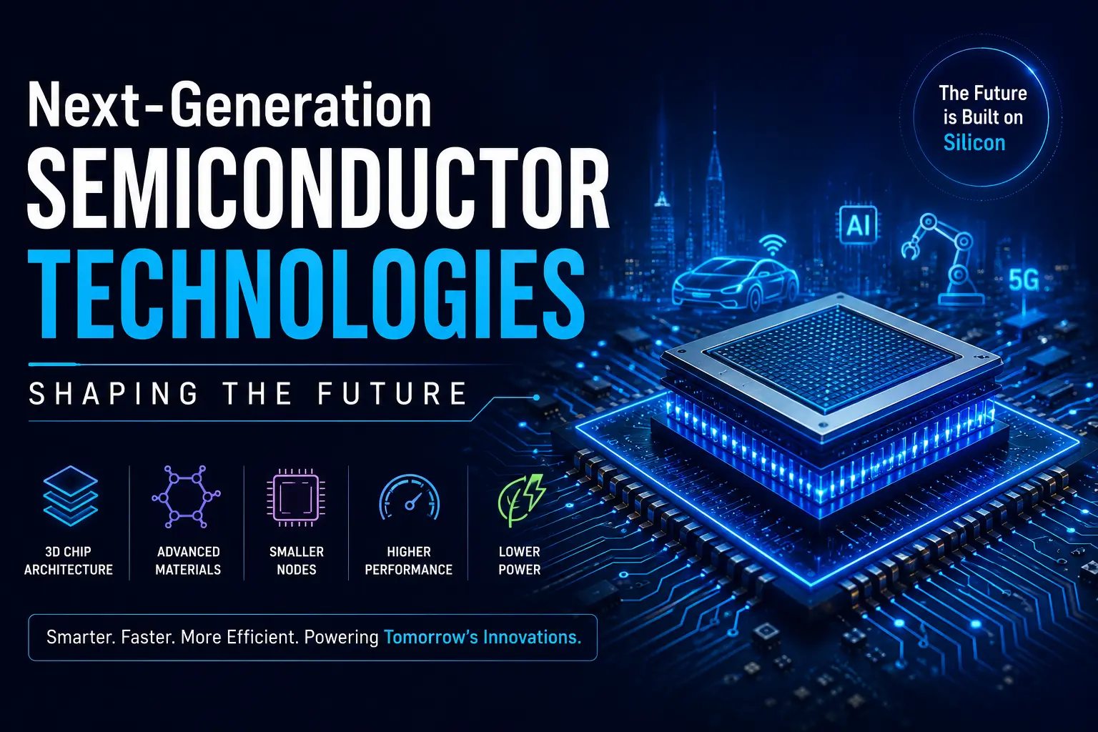
The semiconductor industry is currently undergoing a fundamental transformation. As traditional methods of scaling transistors face physical limits, innovation has pivoted toward entirely new materials, vertical architectures, and specialized designs. In 2026, these advancements are not merely incremental; they are the primary engines powering the next era of artificial intelligence, autonomous systems, and sustainable energy.
Innovations in Architecture and Integration
The era of relying solely on shrinking transistor sizes is shifting toward system-level optimization. Engineers are now focusing on how components interact within a three-dimensional space to maximize performance and energy efficiency.
-
3D Heterogeneous Integration: By stacking processors, memory, and sensors vertically, designers are reducing the distance data must travel. This approach, often utilizing chiplets, minimizes latency and significantly boosts overall computing power.
-
Silicon Photonics: Integrating optical components directly onto silicon chips allows for data transmission via light rather than electricity. This breakthrough addresses bandwidth bottlenecks in high-performance data centers by enabling faster, cooler, and more energy-efficient inter-chip communication.
-
Neuromorphic Architectures: Inspired by the human brain, these chips utilize networks of artificial neurons and synapses. This design is highly efficient for machine learning tasks, consuming a fraction of the power required by traditional general-purpose processors.
-
High Bandwidth Memory (HBM): As AI models grow in complexity, HBM has become critical. This technology stacks memory layers to provide the massive data throughput necessary to keep powerful AI accelerators fed with information without slowing down.
Advancements in Semiconductor Materials
Beyond architecture, the physical composition of semiconductors is evolving. The move toward specialized materials is essential for meeting the high-voltage and high-frequency demands of modern electronics.
-
Wide-Bandgap Materials: Silicon Carbide (SiC) and Gallium Nitride (GaN) are replacing standard silicon in high-power applications. These materials are instrumental in the development of 800-volt electric vehicle architectures and high-efficiency power supplies for AI data centers.
-
Carbon Nanotubes and Graphene: Researchers are leveraging these materials for their exceptional conductivity and thermal properties. They represent the next frontier for high-speed computing, offering potential improvements in both performance and heat dissipation.
-
Advanced Thermal Management: Innovative cooling solutions, such as micro-convective liquid cooling, are being integrated directly into the chip package. This allows chips to run at higher power densities without overheating, removing the need for bulky traditional cooling systems.
The Strategic Shift to Domain-Specific Silicon
The modern computing landscape is bifurcating into general-purpose hardware and highly specialized, application-specific integrated circuits (ASICs). This shift is driven by the specific needs of artificial intelligence and edge computing.
-
Custom AI Accelerators: Rather than relying on standard hardware, major technology players are designing custom silicon tailored to specific algorithms, such as image recognition or large language model inference.
-
Edge Intelligence: By pushing processing power to the “edge”—directly into devices like sensors, robots, and appliances—semiconductors now enable real-time, autonomous decision-making without constant reliance on the cloud.
-
Physical AI: The integration of AI into robots and autonomous industrial systems requires hardware capable of “tacit knowledge” acquisition. Specialized AI chips now process vast amounts of sensor data locally to allow machines to interact with unstructured environments safely and efficiently.
Conclusion
The trajectory of semiconductor technology in 2026 is defined by convergence. The intersection of novel materials like GaN, vertical 3D integration, and AI-optimized architectures is creating a more powerful and efficient digital ecosystem. These developments are the bedrock of human progress, facilitating everything from cleaner energy grids and smarter autonomous vehicles to advanced healthcare diagnostics, ensuring that the technology of the future remains both robust and sustainable.
FAQs
1. Why is the industry moving toward 3D chip integration?
Traditional 2D scaling is reaching physical limits. Stacking components vertically allows for higher packing density, shorter connections, and improved energy efficiency, which is essential for modern high-performance computing.
2. What role do Silicon Carbide and Gallium Nitride play?
These wide-bandgap materials can handle higher voltages and temperatures than traditional silicon. They are vital for the efficiency of electric vehicle powertrains and the power management of AI data centers.
3. What is “Physical AI” and how does it rely on semiconductors?
Physical AI refers to AI systems that operate in the real world, like robots. They require specialized chips capable of processing sensor data and making autonomous, split-second decisions locally at the “edge.”
4. How does silicon photonics improve data center performance?
Silicon photonics uses light instead of electricity to move data between chips. This drastically increases bandwidth and reduces energy loss, solving the connectivity bottlenecks often found in large-scale AI infrastructure.
5. Why are companies investing in custom AI silicon?
Custom chips, or ASICs, are designed for specific tasks like language processing. They offer far better performance-per-watt and lower latency compared to general-purpose processors, which is crucial for training and running complex AI models.